Electrical Double Layer based devices, College of Engineering
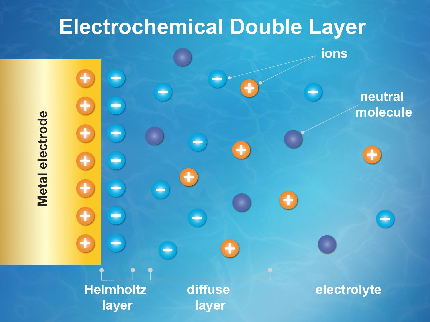
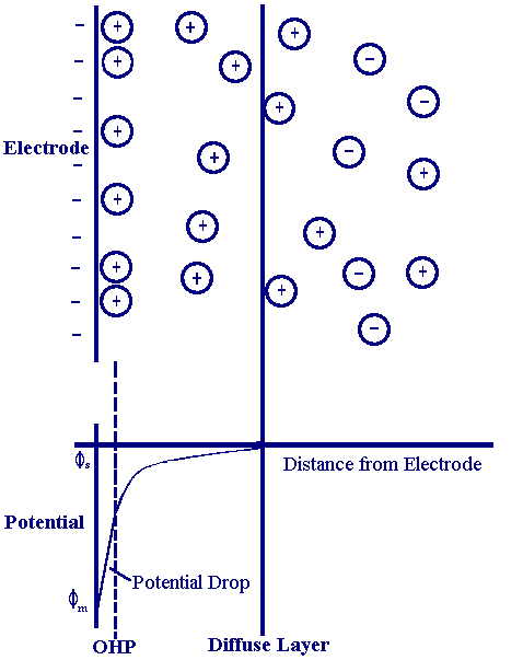
Immersing a metal (electrode) in a salt solution will spontaneously accumulate ions due to image charge to form the well known electrical double layer (EDL). Sign of the charge depends on the Fermi level (i.e., the electrochemical potential) difference between the metal and the solution. For example, gold will accumulate negative ions (i.e., anions). The interfacial structure

PDF) Hybrid Energy Storage in EV with Super Capacitor and Battery MATLAB Simulation

MSc in Electrical and Computer Engineering - Khalifa University

Electrical, School of Engineering

Routing Requirements for a USB Interface on a 2-Layer PCB, Blog

Physicists demonstrate Young's double-slit interference in time – Physics World

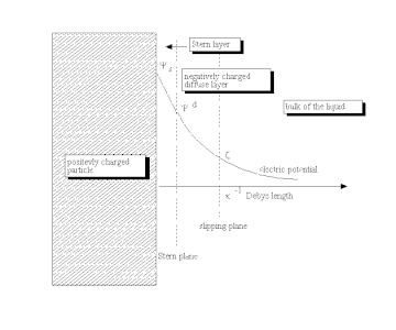
1: Electrical double layer. Depiction of the electrical double layer
The Electrical Double Layer Department of Chemical Engineering and Biotechnology
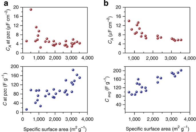
Capacitance of carbon-based electrical double-layer capacitors

Welcome, Department of Electrical and Computer Engineering, College of Engineering
The Electrical Double Layer Department of Chemical Engineering and Biotechnology
Transparent graphene electrodes might lead to new generation of solar cells, MIT News

What is a PCB and PCB Design?

Electrolysis Definition, Reaction & Process - Lesson

What is an Electric Double Layer? – Gebbie Lab – UW–Madison