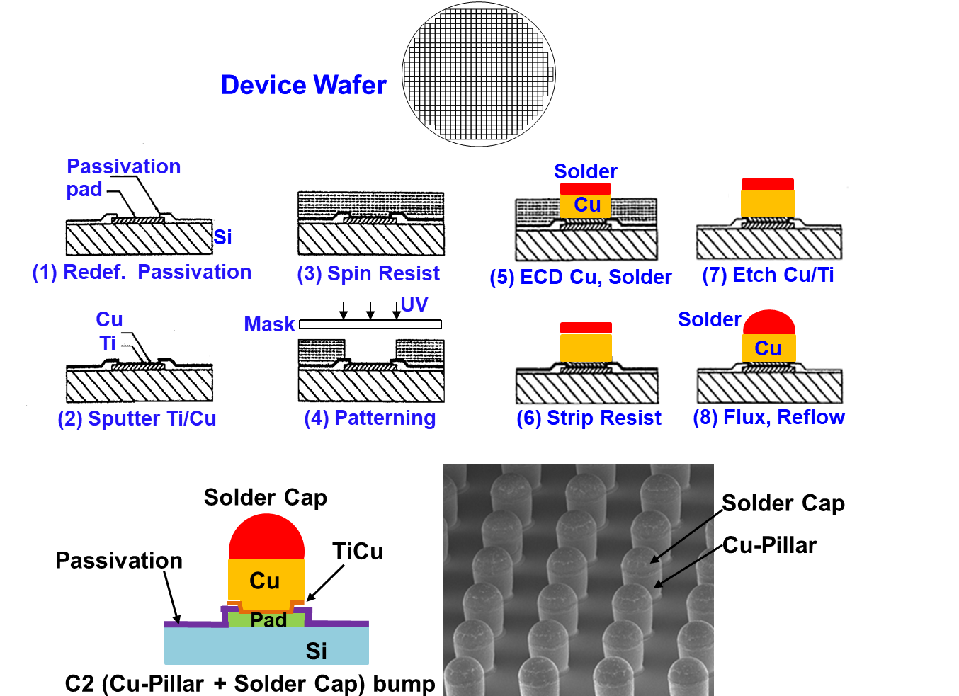
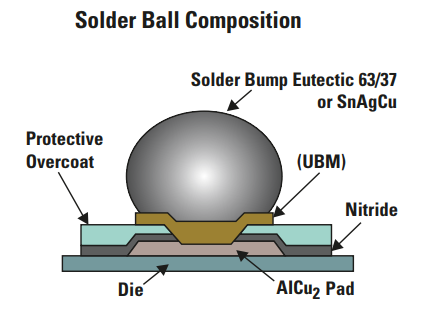
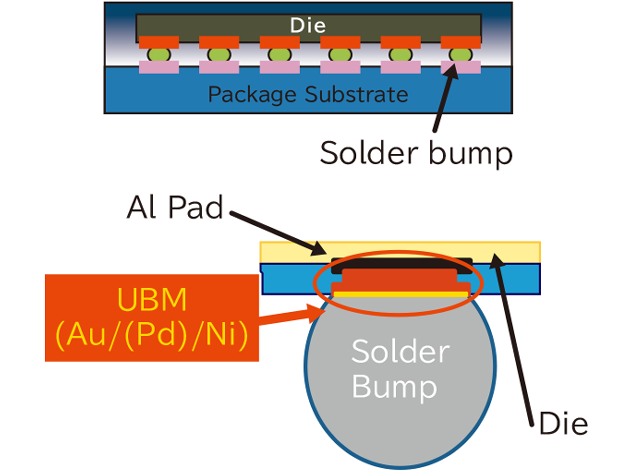
UBM (under bump metallurgy) structure

Description

Kyung-Wook PAIK Korea Advanced Institute of Science and

PDF) Eutectic Pb/Sn solder bump and Under Bump Metallurgy
Scaling Bump Pitches In Advanced Packaging

PDF) Eutectic Pb/Sn solder bump and Under Bump Metallurgy
High Performance Electroless Nickel that's Lead and Cadmium-Free

The surface characteristics of under bump metallurgy (UBM) in electroless nickel immersion gold (ENIG) deposition - ScienceDirect

PDF) Under Bump Metallurgy (UBM)-a technology review for flip chip packaging

Schematic structures of the cross-section of the indium bump just
TPS82130: difference of the internal structure between NanoStar(WCSP) and PicoStar - Power management forum - Power management - TI E2E support forums
Related products


$ 15.50USD
Score 4.9(487)
In stock
Continue to book
$ 15.50USD
Score 4.9(487)
In stock
Continue to book
©2018-2024, farmersprotest.de, Inc. or its affiliates