pcb - What is the pad size required for this BGA AW H3 Chip? - Electrical Engineering Stack Exchange

I'm trying to figure out the pad size to use for my footprint according to this datasheet.The last page in the datasheet has the package dimensions. I've also posted the relevant information in a p

Page 14 – RAYPCB

BGA Pad Size Deep Dive Component Creation
How to Create a SMD pad using the Allegro Padstack Editor? - PCB Design Tutorial - PCBway
What is a Pad in PCB Design and Development
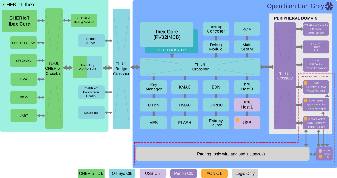
lowrisc.github.io/index.xml at master · lowRISC/lowrisc.github.io · GitHub

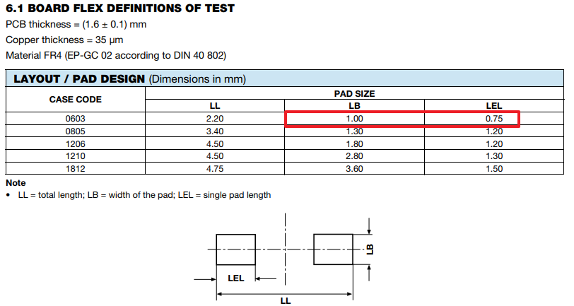
pcb design - I have a doubt on taking pad dimensions in this below picture what is the pad width and height.any body kindly clear my doubt - Electrical Engineering Stack Exchange

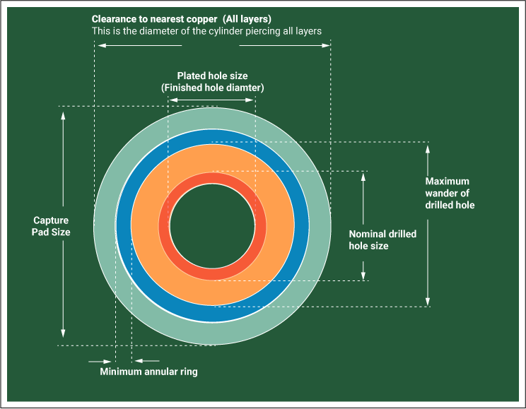
pcb design - Recommended Pad Layout Hole Size - Electrical Engineering Stack Exchange

ADSP-BF512/4/6/8(F16) Datasheet by Analog Devices Inc.

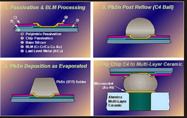
Silicon Exposed: BGA process notes

PDF) Complete PCB design using orcad_capture and layout
BO23EB-11 Unified Namespace